In Memory Computing approaches
Memory centric architectures can
be associated to many topologies
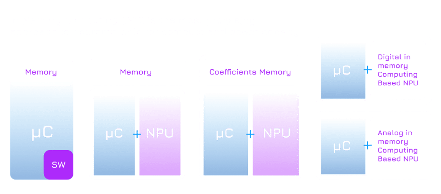
Two broad classifications of IMC apply: DIMC (Digital In Memory Compute) and AIMC (Analog In memory Compute)
In the case of DIMC the computation happens in the memory spread across the single memory bit cell and a group of bit cells that can be accessed in parallel to perform an accumulation operation. This deterministically generates a precise bit accurate output.
The AIMC architectures are associated to cases where the computation happens by way of an analog operation such as a current summation or charge transfer either in a column wise or a row wise fashion with an analog and digital conversion at the end to generate the final output
In NeuroSoC the focus will be on AIMC.
Objectives
Detailed technical objectives
- Design of a PCM computational memory tile for AIMC in 28nm FD-SOI technology
- Design of a SRAM computational memory tile for AIMC in 28nm FD-SOI technology complementing the PCM one for selected ultra-low cost and always on use-cases
- Design of a reusable and modular hybrid IMC based neural processing unit for scalable edge-AI SoCs
- Assessment and characterization of security exploits techniques for IMC based NPUs
- Enhancement of a RISC-V multicore microcontroller implementation to support functional safety
- Explore functional safety solutions for IMNPU IPs for industrial and automotive use cases
- Study and optimize AI Deep Learning algorithms optimized for IMC and selected use-cases
- Prototype IMC based AI tools and compilers for efficient mapping of deep learning algorithms
- Design of an advanced 28nm FD-SOI complete MPSoC integrating the technology developed in the project
- Validate use-cases to assess the benefits of the technology and tools developed in the project
NeuroSoC achievements after 12 Months
In the first year of the project, the focus of the work has been the definition of the hardware architecture and the various elements needed, with a special focus on the development of a PCM NVM memory capable to store multilevel values, and to perform In Memory Computing.
For the IMNPU unit, three distinct architectures, namely the router-based, cluster-based and 2D mesh-based architectures, were evaluated for their suitability for the targeted weight stationary system. More specifically, the architectures were assessed for design flexibility, scalability, performance/cost and power efficiency. Finally, the 2D mesh-based architecture was selected as a suitable candidate for NeuroSoC. Various approaches to schedule the data processing in the mesh architecture have been discussed with the conclusion that two schemes, the time scheduling approach and the data driven approach provide advantages for specific use cases. The evaluation of these approaches brought the conclusion that both approaches seem to have their advantages and disadvantages. Since the implementation of the required hardware support for both schemes is negligible, we decided to support both schemes and to provide the software tool chain with the freedom to use one or the other depending on the use case and better applicability. The initial version of the RISC-V component has been synthesized in various configurations.
Regarding the security aspects, two methods, the “Encoder-Decoder based approach” and the “Tile-by-Tile approach” have been successfully explored, showing potential security risks on the In-Memory Computing (IMC) based systems due to Side-Channel Attacks.
For the characterization of the PCM cell, a set of different type of cells have been considered, and two batches of standard and rheostatic cells have been fabricated and extensively characterized.
On these cells, a multilevel programming algorithm has been implemented. With the results obtained in the first period, the multilevel is working, but convergence is not always guaranteed. The algorithm and the convergence are under refinement. The computational accuracy of the Analog In Memory Computing based on PCM , and the comparison with the digital compute engine are under evaluation.
For the design of the AIMC tile, two architectures have been considered, one main architecture and one exploratory architecture, both starting from elements of existing tiles from IBM and ST.
A RTL design of the AIMC tile, to be integrated in the overall architecture, has been realized, and it is ready to be produced for the verification of the real hardware.
For the AIMC based on SRAM, a first test chip has been realized and it is currently under evaluation in terms of non idealities of the real hardware and effect of analog noise sources.
Finally a first version of the wrapper of the AIMC tiles in the main architecture has been defined.
Regarding the development of the software toolchain to be used to program the NeuroSoC system, based on the hardware architecture that has been depicted during the first year, the software stack components have been identified and connected in a proper structure, in order to allow the deployment of neural networks on the emulator first, and finally on the NeuroSoC device. In the first year the focus has been on the definition of the software architecture and the related simulations/emulation elements, taking into consideration the needs of the end user for the demonstration of efficiency and quality level requirements.
Based on the variety of applications considered, from automotive to aerospace, security and safety, the requirements of the target applications of the NeuroSoC device have been analyzed and the possibility of fulfillment of these requirements with the defined architecture has been confirmed.
Non confidential summary of confidential deliverables can be found below.
D1.1 FD-SOI 28nm PCM existing multilevel cell characterization
With the wider diffusion of AI applications both at system level and at the edge, the demand for performance of integrated devices is growing more and more. Most important area of improvement are recognized in terms of power consumption and speed. In fact, the computational complexity of Neural Network (NN) is in the resolution of several linear systems that require a large amount of power
and time to execute all operations. In the Von-Neumann classical system architecture, the CPU must elaborate every sum and multiplication transferring data from/to memory several times through the communication bus. This causes a significant loss in terms of power and speed. The response to these issues could be found in in-memory computing (IMC) technologies. Resistive memory
matrices, due to their conformation, lend themselves well to the possibility of carrying out Matrix-Vector-Multiplication (MVM) operations in a simple way (and with a single clock’s cycle).
Among the resistive memories, one of the most promising candidates is undoubtedly the PCM. In literature could be found many research papers and proposing PCM technology as resistance-based memory array to implement an IMC solution. Almost all of them use the classic unconfined cell architectures typical of embedded or stand-alone memories (Wall or Mushroom architectures). The aim of this deliverable is to present the PCM Rheostatic cell technology developed to overcome the limitations, when used for AIMC neuromorphic accelerators, of the conventional PCM cell architectures widely adopted for digital memory applications.
Extensive characterization of the PCM Rheostatic AIMC cell, including the MOS selector, supported by TCAD model results, is reported. Compact model of the optimized cell is also included. A statistical evaluation performed at test chip level on conventional Wall cell architecture (since test chip with Rheostatic cell is not yet available), aimed to study the best strategy to limit the LRS conductance,
has finally been reported.
D1.2 Final PCM optimized multilevel cell characterization and initial statistical evaluation
Lab based electrical measurements were performed on a standard multi-megabits memory arrays (not IMC arrays) mapped on silicon test vehicles by STMicroelectronics at the beginning of the project. This will drive the design and analysis of optimized programming algorithms required to program the PCM devices to target conductance levels and to identify the appropriate current profiles to specify the analog circuits. The array-level measurements will also facilitate the development of statistical models of the time/temperature dependence of conductance distributions which will support the algorithmic exploration.
D2.1 PCM AIMC tile architecture specifications
The objective of WP2 is to design an analog in-memory computing, AIMC, tile. The tile comprises a crossbar array of “unit cells”. Each unit cell comprises one or more phase-change memory, PCM, devices and stores the synaptic weights corresponding to a deep neural network layers in terms of the analog conductance value of the PCM devices. The tasks within this work package involve defining the unit cell and a suitable array structure and designing the associated digital and analog circuits to feed digital input data into the array. Such an array can perform the analog equivalent of matrix-vector multiplication, MVM, operations, produce results (in terms of currents or voltages), and convert them back to digital domain with suitable ultra-low power circuits such as digital-to-analog converters, DACs, analog-to-digital converters, ADCs, and peripheral circuits.
The objective of this deliverable is the analysis of different possible implementations of the tile architecture.
D2.2 RTL model of PCM AIMC tile with periphery
The objective of WP2 is to design an analog in-memory computing tile. The tile comprises a memory array of “unit cells”. Each unit cell comprises one or more phase-change memory devices and stores the synaptic weights corresponding to a deep neural network layers in terms of the analog conductance value of the PCM devices. The tasks within this work package involve defining the unit cell and a suitable array structure and designing the associated digital and analog circuits to feed digital input data into the array. Such an array can perform the analog equivalent of matrix-vector multiplication operations, produce results (in terms of currents or voltages), and convert them back to digital domain with suitable ultra-low power circuits such as digital-to-analog converters analog-to-digital converters and peripheral circuits.
The objective of this deliverable is to report about the AIMC tile, from now on defined as AIMC IP, model purpose, its functionalities, and its usage.
D3.2 Multi-tile IMNPU specifications and IP synthesizable functional model
The objective of this deliverable is to provide the first version of the IMNPU architecture and NeuroSoC system design. Moreover, the deliverable describes in detail different units in the provisioned IMNPU and their first version specifications. The deliverable also includes the first version of RTL implementation or synthesis results of the main units.
D3.3 Initial assessment of security vulnerabilities
The main goal of this deliverable is to conduct a comprehensive investigation of hardware-level security vulnerabilities that arise in in-memory-based neural network inference as envisioned in the NeuroSoC project. Special emphasis is placed on the potential for Side-Channel Attacks (SCA), which pose a significant threat to the confidentiality of the neural network’s configuration and parameters. These parameters, particularly the neural network model’s weights, encapsulate the knowledge the model has learned during training. The weights hold valuable proprietary information, the leak of which could potentially expose sensitive data, or allow malicious entities to
copy or reverse-engineer the model. Moreover, creating a good dataset for model training is often a challenging, time-consuming, and expensive task.
Hence, the weight parameters effectively represent a significant investment of resources. In cases where models are trained on sensitive data, such as personal health information or confidential business data, unauthorised access to weights can lead to serious privacy breaches. Power analysis attacks, in particular, exploit the correlation between power consumption and the operations performed by the hardware, making them a potent vector for extracting sensitive information like these weights. This makes power analysis attacks a particularly insidious threat, as they bypass traditional software-based security measures and directly target the physical characteristics of the hardware. Therefore, safeguarding these weights against power analysis attacks is crucial to maintain data confidentiality, preserve resource investments, and even though the privacy of the weights in the model is achieved for SCA, data integrity can still be compromised.
D5.3 Competitors, benchmarks and KPIs report
In 2014, the first dedicated Vision Processing Unit (VPU) was introduced, sparking an explosion in the market for edge AI products. Today, a wide variety of vendors offer products at different performance levels, ranging from ultra-low power speech AI chips to high-performance units that can seamlessly replace desktop GPUs. AI silicon architectures can be grouped into five broad categories: GPUs, streaming VPU architectures, dedicated solutions for verticals, programmable silicon products, and single vertical silicon.
This report presents the benchmarks required for a novel state-of-the-art edge AI accelerator, as identified by potential customers and partners. A survey of the edge AI accelerator landscape is also presented, based on published benchmark data of competitors. In consultation with NeuroSoC partners, the report proposes specific neural network architectures for benchmarking the NeuroSoC chip based on the trends and needs of industry. The report also discusses the use cases influencing these choices and the rationale for choosing them.
A set of industry based Key Performance Indicators (KPIs) are proposed to provide a benchmark for the NeuroSoC chip. On the software side, the requirements needed for NeuroSoC to be a competitive solution have also been outlined within this report.
Overall, this report provides a comprehensive overview of the current landscape of edge AI accelerators and outlines the benchmarks and KPIs required for a novel state-of-the-art edge AI accelerator like the NeuroSoC chip. It also highlights the importance of a functional and easy-to-use toolchain for the chip to be competitive in the market.
D5.4 First NeuroSoC emulator performance report
The design of the NeuroSoC chip will be available at the last year of the project. For being able to analyze different DNN models on how they can be ported in the NeuroSoC chip, before the chip becomes available, the NeuroSoC Emulator has been developed. The NeuroSoC Emulator is a system of hardware components and software tools, covering all phases for mapping and executing a DDN model. The NeuroSoC Emulator allows us to study the effect of PCM technology on the accuracy of these models, to develop microcode end applications, and the complete data flow from an AI model to the hardware configuration files, resulting to an inference engine where the model is executed. These Emulator’s capabilities are based on accurate functional emulation of the NeuroSoC chip components, supporting testing and co-implementation.
The NeuroSoC Emulator consists of several reconfigurable boards organized in a distributed environment and interconnected using high speed links. The NeuroSoC Emulator provides an accurate emulation environment of the NeuroSoC chip, with advanced debugging and statistical analysis capabilities.